Industrial Consultancy & Sponsored Research (IC&SR) , IIT Madras
PCB-incorporated based low cost differential mode filter for EMI/ EMC of power electronic converter
Technology Category/Market
Technology: A hybrid analog to digital converter and method
Category: Electronics & Circuits
Industry: Electronic System & Design Manufacturing (ESDM), Robotics
Application: Analog to Digital converter
Market: The global market size is expected to grow at a CAGR of 6.3% during 2022-2030, to surpass US$ 6.29 Billion by 2030.
Image Gallery
Problem Statement
- Electromagnetic interference (EMI) poses significant challenges for power electronic converters, necessitating emissions below international standards.
- The frequency range for conducted emission noise in power electronics is 150 kHz to 30 MHz, divided into high-frequency and low-frequency zones.
- Low-frequency zone primarily influences conducted emissions due to converter switching frequency.
- High-frequency zone includes emissions related to switching transients, especially in Wide Band Gap devices like SiC MOSFETs.
- Current passive filter designs typically maintain a corner frequency below 150 kHz.
- PCB-level inductors are utilized in series with X-capacitors, optimizing impedance at around 160 kHz.
- Biela et al. (2009) present a passive hybrid integrated EMI filter, combining integrated and discrete components.
- Despite advancements, reliance on bulky common mode chokes and differential mode inductors remains a limitation, especially in achieving inductors with high self-resonant frequency values.
Technology
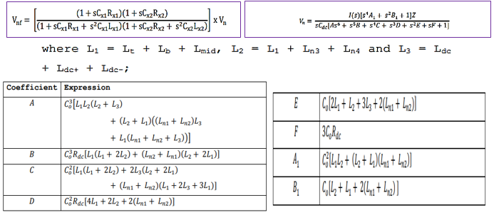
A filter reduces Differential Mode (DM) emission noise in power converters with an inductance-capacitor circuit and damping resistance, ensuring attenuated noise (Vnf) meets the equation.
Key Features/Value Proposition
Reducing Differential Mode Emission Noise in Power Converters:
- Utilizes printed circuit board filter.
- Implements inductance-capacitor circuit with damping resistance.
- Adjusts length, width, thickness, and distance between PCB traces.
- Multi-layer PCB for higher inductance and current rating.
- Device free from magnetic core.
- Estimates differential mode noise voltage for voltage source inverter.

Questions about this Technology?
Contact for Licensing
Research Lab
Prof. Kamalesh Hatua
Department of Electrical Engineering
Intellectual Property
IITM IDF Ref. 2524
Patent No: IN 549282
Technology Readiness Level
TRL-6
Technology validated in relevant environment (Industrially relevant enabling technologies)
